|
CAFC判決
Collabo
Innovations Inc., v. SONY Corporation
2020年2月25日
URL
LINK
OPINION
by JUDGE PROST,
Chief
Judge, LOURIE
Dissenting
in Part by CLEVENGER
Summarized
by Tatsuo YABE – 2020-03-06
|
|
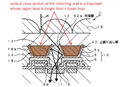
本事案はPTABのIPR手続きからの控訴事件である。本事件には複数の争点があるが、そのうちの一つであり唯一PTABで意見が分かれたのは従属クレーム3の自明性判断であった。しかしPTABの多数意見(審決)では従属クレーム3も自明であると判断した(反対意見有り)。依ってCollaboのUSP7023034特許のクレームは全て無効となった。CAFCでの争点の一つを一言で云えばクレーム3の特徴(上辺が下辺よりも長い台形状の反斜壁)がAbe引例の図3に開示されていると理解できるか否かであった。
|
|
クレーム3(サポート:図6;コラム9、10-22行目)
|
Abe引例の図3
|
|
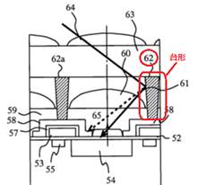
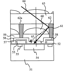
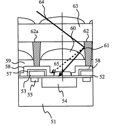
62:上辺が下辺よりも長い台形状の反斜壁
Claim 3:
a vertical cross section
of the reflecting wall (62) is a trapezoid whose upper base is longer than
a lower base.
|
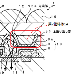
1: CCD個体撮像素子
9:第2遮光膜
10:遮光膜
14:第2絶縁体
|
|
PTABの意見は分かれたが多数意見(即ち審決)としてAbe引例の図3に開示された構造は全体として台形であると判断した。当該判断(事実審)を不服とし控訴されたがCAFCはPTABの判断は実質的な証拠(substantial
evidence)に基づくとして審決を支持した(SONYの勝訴)。
|
・・・ではあるが、ここでCollaboはUSP7023034の権利を全て失うとは限らない。Collaboは再審査手続きで反斜壁62の材料が同一部材で構成されているとか、反斜壁62の上面が水平であるとかに限定することで自身の特許を維持することは可能である。(以上筆者)
|
■
事件の背景:
CollaboはUSP
7,023,034特許を所有しており、当該特許に対してSONYがPTABでIPR手続きを開始した。 PTABは3名の行政判事全員合意で034特許のクレーム1-2,
4-11, 13-18は自明で無効と判断した。しかし、クレーム3と12に関しては2:1で自明、Anderson行政判事は自明性に反対した。Collaboは第1の争点としてクレームの反斜壁(reflective
wall)の解釈を不当に広く解釈しているとしPTABの判断の取消しを求め、第2争点としてクレーム3と12の特徴はAbe引例には開示されていないとしてCAFCに控訴した。
|
■
特許権者: Collabo
■
特許:USP No. 7,023,034(以下034特許)
■
IPR申請人: SONY
■
特許の概要:
034特許はマトリックス状に配列された複数の感光体を備えた固体状の画像形成装置に関する。本事案で問題となった特徴は、感光体同士を仕切るために個々の感光体(Photo
Diode 54)に設けられた一対の反斜壁であり、当該反射壁(62)の断面形状である。USP034の図2では反射壁の断面形状が長方形であるが、図6には反射壁の断面形状が台形のものが開示されている。この図6で開示された反射壁(62)の断面形状が従属クレーム3と従属クレーム12で規定された。
|
|
■ PTABの判断:
034特許のクレーム1-2,
4-11, 13-18は自明で無効。しかし、クレーム3と12に関しては2:1で自明、Anderson行政判事は自明性に反対。
|
■ 争点:
第2争点に関してのみ述べる(筆者)
従属クレーム3(及び従属クレーム12)の特徴「反射壁の垂直断面における形状は上面が下面よりも長い台形である」がAbe引例(JPH11-087674
)の図3に開示されていると理解できるか? 上記のようにPTABでは2名の判事はAbe引例の図3より当該特徴を読み取れると解釈(多数意見)したが、1名は反対であった。
|
|
Claim 3 (Claim 12):
|
The solid-state imaging
device according to claim 1, wherein a vertical cross section of the
reflecting wall is a trapezoid whose upper base is longer than a lower
base.
反射壁の垂直断面における形状は上面が下面よりも長い台形である
|
|
FIG. 6
|
明細書のサポート
|
|
|
Also, a cross section of the reflecting wall of the
solid-state imaging device according to the present embodiment is
rectangular as shown in FIG. 2, but it is not limited thereto. For
example, as shown in FIG. 6, a cross section of
the reflecting wall may be a trapezoid whose upper base is longer than the
lower base. As a result, as shown in FIG. 6, it is possible to
further efficiently collect the oblique light onto the aperture. Further,
the bottom of the reflecting wall is narrower than the bottom of the
reflecting wall shown in FIG. 2, whereby it is possible to substantially
move the reflecting wall from side to side. As a result, design freedom of
the solid-state imaging device is increased.
|
|
■ CAFCの判断:
CAFCは、下級審(PTAB)の事実判断に対してはsubstantial
evidence(実体的な証拠を基礎として事実審理が行われたか否か)の基準で判断する。
|
CAFCはSONYの主張とCollaboの主張をレビュし、SONYの主張を認めたPTABのMajority
Opinionに同意した。
|
◇
SONYの主張
Abe引例の図3に開示されているように反斜壁の先端部92は上方向に傾斜し延設し、下図の茶色で示すように全体として台形(上が下よりも長い)である。
|
|
◇
Collaboの主張
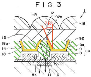
CollaboはAbe引例の図3を以下のように追記し、Abe引例の図3にクレーム3で規定する台形は開示されていないと主張した。以下図3で示す緑色の部分14は透明の絶縁体である。反斜壁9は上面に相当する部分がなく、寧ろ、上方向に開口したU形状、カップ形状、或いは、お椀形状であって台形ではない。
|
|
PTABは上記当事者の主張を勘案した結果、多数意見(2:1)はSONYの主張に同意した。Abe引例の図3に開示されているものは、カップ型の構造であり全体(カップの内部のMaterialも含めて)として台形状の反斜壁と理解できると解釈した。
After weighing both parties’ positions, the
Board found that Abe does disclose a trapezoid. Citing Sony’s petition, as
well as the same portions of Abe cited in Sony’s petition, the Board
determined that “the entire cup shaped structure, including the material
within, is the recited ‘reflecting wall.’”
|
CAFCはPTABの多数意見を支持した。即ち、Abe引例の図3には四辺形の構造が開示されており、その下部は横方向に延設する遮光フィルム9の下部であり、上面は第2絶縁フィルム14(遮光フィルム9の内部に存在する絶縁フィルム14)の上面で構成され、14の上面部は遮光フィルム9の下部よりも長いと読み取れる。然るに、PTABの多数意見(Abe引例は上面が下面より長い台形状の反斜壁を開示している)は実質的な証拠でサポートされている。
Figure 3 of Abe, on its face, discloses a
trapezoidal shape. As the Board described, it shows a quadrilateral bounded by
the lateral faces of light shielding film 9, the bottom surface of light
shielding film 9, and the top surface of second insulating film 14 within the
interior of light shielding film 9. -958 Decision at 41 (citing Abe ¶¶
38–39). The top surface, made of a portion of second insulating film 14,
is longer than the bottom surface of light shielding film 9. Abe undisputedly
discloses that the lateral faces of the light shielding film 9 reflect light. See
Appeal No. 19-1152 J.A. 937 (Collabo’s expert referring to light shielding
film 9 as a “reflector”). Therefore, we hold that substantial evidence
supports the Board’s conclusion that Abe discloses “a vertical cross section
of the reflecting wall is a trapezoid whose upper base is longer than a lower
base.”
|
■
References:
|
Claims 1, 3, 10 and 12 of USP 7,023,034
|
1. A solid-state imaging device comprising:
a semiconductor substrate;
a photoreceiving region provided on the semiconductor substrate;
a plurality of light-sensitive elements provided in the photoreceiving region;
a plurality of apertures, which are provided over the light-sensitive elements,
for delivering an incident light to the light-sensitive elements;
a plurality of reflecting walls formed over the light-sensitive elements and the
apertures so as to oppose each other across the apertures; and
a plurality of micro lenses provided over the reflecting walls and the
apertures,
wherein the plurality of micro lenses disposed in an inner periphery of the
photoreceiving region, and the plurality of reflecting walls corresponding to
the micro lenses are disposed such that a center of each of the micro lenses and
a center of each of the reflecting walls opposing each other are displaced from
a center of the aperture toward a center of the photoreceiving region, and
an amount of displacement between the center of the photoreceiving region and
the center of the reflecting walls is smaller than that of displacement between
the center of the photoreceiving region and the center of the micro lens.
|
3. The solid-state imaging device according to claim 1, wherein a vertical cross
section of the reflecting wall is a
trapezoid whose upper base is longer than a lower base.
|
10. A solid-state imaging device comprising:
a semiconductor substrate;
a photoreceiving region provided on the semiconductor substrate;
a plurality of light-sensitive elements provided in the photoreceiving region;
a plurality of apertures, which are provided over the light-sensitive elements,
for delivering an incident light to the light-sensitive elements;
a plurality of reflecting walls provided over the light-sensitive elements and
the apertures so as to oppose each other across the apertures;
a plurality of a first micro lenses provided between the reflecting walls; and
a plurality of a second micro lenses provided over the reflecting walls and the
apertures,
wherein the plurality of the first and second micro lenses disposed in an inner
periphery of the photoreceiving region, and the plurality of reflecting walls
corresponding to the first and second micro lenses are disposed such that a
center of each of the first micro lenses, a center of each of the second micro
lenses, and a center of each of the reflecting walls opposing each other are
displaced from a center of the aperture toward a center of the photoreceiving
region, and
an amount of displacement between the center of the photoreceiving region and
the center of the reflecting walls, an amount of displacement between the center
of the photoreceiving region and the center of the first micro lens are smaller
than that of displacement between the center of the photoreceiving region and
the center of the second micro lens.
|
12. The solid-state imaging device according to claim 10, wherein a vertical
cross section of the reflecting wall is a
trapezoid whose upper base is longer than a lower base.
|